- 您现在的位置:买卖IC网 > Sheet目录3753 > ATMEGA169P-16MCHR (Atmel)MCU AVR 16KB FLASH 16MHZ 64-VQFN
2005 Microchip Technology Inc.
Preliminary
DS41265A-page 237
PIC16F946
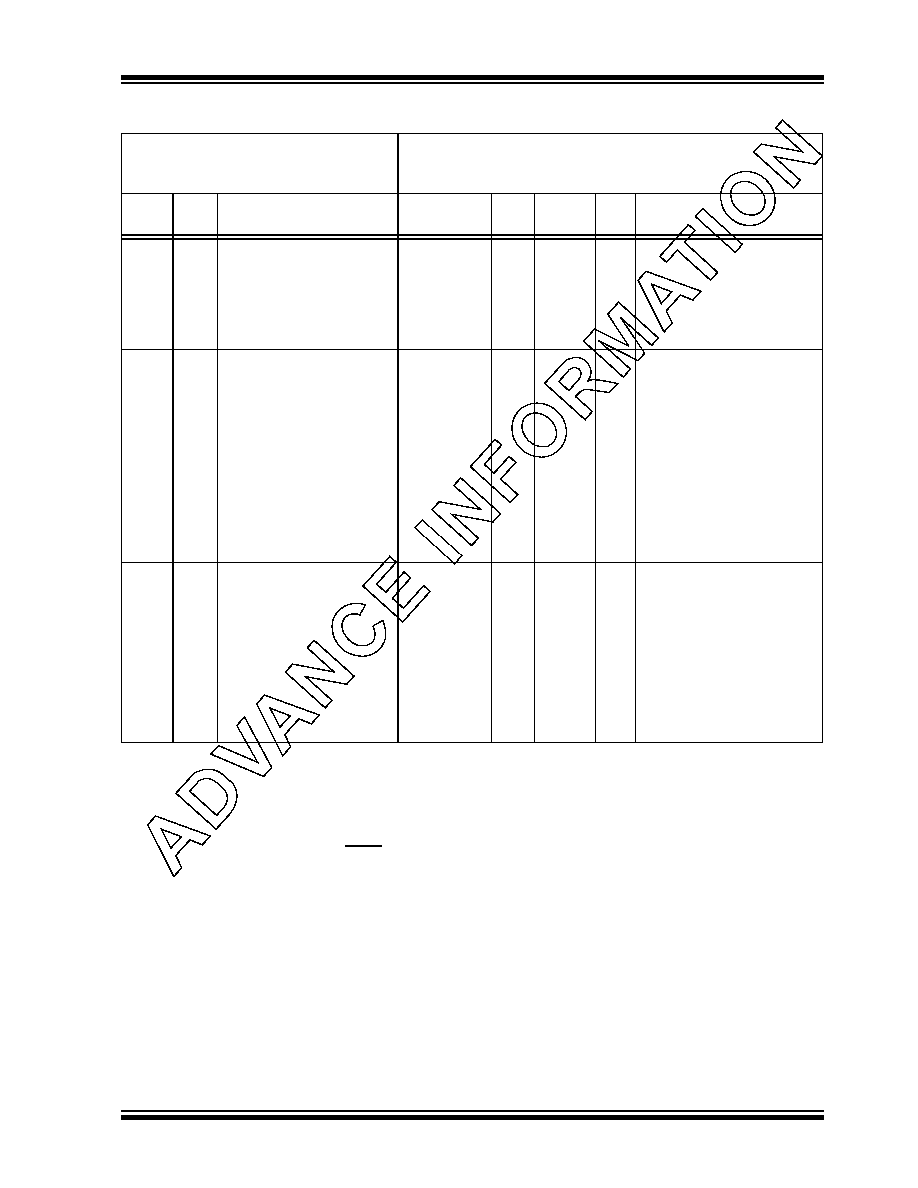
Capacitive Loading Specs
on Output Pins
D100
COS
C2
OSC2 pin
—
15*
pF
In XT, HS and LP modes
when external clock is used to
drive OSC1
D101
CIO
All I/O pins
—
50*
pF
Data EEPROM Memory
D120
ED
Byte Endurance
100K
1M
—
E/W -40
°C ≤ TA ≤ +85°C
D120A ED
Byte Endurance
10K
100K
—
E/W +85°C
≤ TA ≤ +125°C
D121
VDRW VDD for Read/Write
VMIN
—
5.5
V
Using EECON1 to read/write
VMIN = Minimum operating
voltage
D122
TDEW Erase/Write Cycle Time
—
5
6
ms
D123
TRETD Characteristic Retention
40
—
Year Provided no other specifica-
tions are violated
D124
TREF
Number of Total Erase/Write
Cycles before Refresh(2)
1M
10M
—
E/W -40
°C ≤ TA ≤ +85°C
Program Flash Memory
D130
EP
Cell Endurance
10K
100K
—
E/W -40
°C ≤ TA ≤ +85°C
D130A ED
Cell Endurance
1K
10K
—
E/W +85°C
≤ TA ≤ +125°C
D131
VPR
VDD for Read
VMIN
—5.5
V
VMIN = Minimum operating
voltage
D132
VPEW VDD for Erase/Write
4.5
—
5.5
V
D133
TPEW Erase/Write cycle time
—
2
2.5
ms
D134
TRETD Characteristic Retention
40
—
Year Provided no other specifica-
tions are violated
19.4
DC Characteristics: PIC16F946-I (Industrial), PIC16F946-E (Extended) (Continued)
DC CHARACTERISTICS
Standard Operating Conditions (unless otherwise stated)
Operating temperature
-40°C
≤ TA ≤ +85°C for industrial
-40°C
≤ TA ≤ +125°C for extended
Param
No.
Sym
Characteristic
Min
Typ
Max
Units
Conditions
*
These parameters are characterized but not tested.
Data in ‘Typ’ column is at 5.0V, 25
°C unless otherwise stated. These parameters are for design guidance only
and are not tested.
Note 1:
In RC oscillator configuration, the OSC1/CLKI pin is a Schmitt Trigger input. It is not recommended to use an
external clock in RC mode.
2:
Negative current is defined as current sourced by the pin.
3:
The leakage current on the MCLR pin is strongly dependent on the applied voltage level. The specified levels
represent normal operating conditions. Higher leakage current may be measured at different input voltages.
发布紧急采购,3分钟左右您将得到回复。
相关PDF资料
2-1546217-0
TERM BLK RCPT 20POS SIDE 5.08MM
1-1546217-9
TERM BLK RCPT 19POS SIDE 5.08MM
1-1546217-8
TERM BLK RCPT 18POS SIDE 5.08MM
1-1546217-7
TERM BLK RCPT 17POS SIDE 5.08MM
1-1546217-6
TERM BLK RCPT 16POS SIDE 5.08MM
1-1546217-5
TERM BLK RCPT 15POS SIDE 5.08MM
1-1546217-4
TERM BLK RCPT 14POS SIDE 5.08MM
1-1546217-3
TERM BLK RCPT 13POS SIDE 5.08MM
相关代理商/技术参数
ATMEGA169P-16MCU
功能描述:8位微控制器 -MCU AVR 16KB, 512B EE 16MHz 1KB SRAM, 5V
RoHS:否 制造商:Silicon Labs 核心:8051 处理器系列:C8051F39x 数据总线宽度:8 bit 最大时钟频率:50 MHz 程序存储器大小:16 KB 数据 RAM 大小:1 KB 片上 ADC:Yes 工作电源电压:1.8 V to 3.6 V 工作温度范围:- 40 C to + 105 C 封装 / 箱体:QFN-20 安装风格:SMD/SMT
ATMEGA169P-16MU
功能描述:8位微控制器 -MCU AVR 16K FLASH 512B EE 1K SRAM LCD ADC RoHS:否 制造商:Silicon Labs 核心:8051 处理器系列:C8051F39x 数据总线宽度:8 bit 最大时钟频率:50 MHz 程序存储器大小:16 KB 数据 RAM 大小:1 KB 片上 ADC:Yes 工作电源电压:1.8 V to 3.6 V 工作温度范围:- 40 C to + 105 C 封装 / 箱体:QFN-20 安装风格:SMD/SMT
ATMEGA169P-16MU SL383
制造商:Atmel Corporation 功能描述:MCU 8BIT ATMEGA RISC 16KB FLASH 3.3V/5V 64PIN MLF - Tape and Reel
ATMEGA169P-16MUR
功能描述:8位微控制器 -MCU AVR LCD 16KB FLSH EE 512B 1KB SRAM-16MHZ RoHS:否 制造商:Silicon Labs 核心:8051 处理器系列:C8051F39x 数据总线宽度:8 bit 最大时钟频率:50 MHz 程序存储器大小:16 KB 数据 RAM 大小:1 KB 片上 ADC:Yes 工作电源电压:1.8 V to 3.6 V 工作温度范围:- 40 C to + 105 C 封装 / 箱体:QFN-20 安装风格:SMD/SMT
ATMEGA169P-8AU
制造商:ATMEL 制造商全称:ATMEL Corporation 功能描述:Microcontroller with 16K Bytes In-System Programmable Flash
ATMEGA169P-8MU
制造商:ATMEL 制造商全称:ATMEL Corporation 功能描述:Microcontroller with 16K Bytes In-System Programmable Flash
ATMEGA169PA
制造商:ATMEL 制造商全称:ATMEL Corporation 功能描述:8-bit Microcontroller with 16K Bytes In-System Programmable Flash
ATMEGA169PA_1
制造商:ATMEL 制造商全称:ATMEL Corporation 功能描述:High Endurance Non-volatile Memory segments